Problem
One inspection label can hide very different coverage
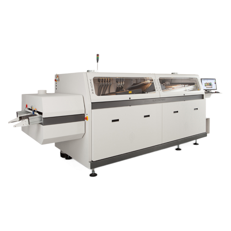
After wave soldering, a mixed assembly may combine through-hole pins, DIP packages, SMD parts, tall components, reflective solder, shadowed regions and bottom-side features. The practical problem is not whether an AOI can find defects in general. It is whether the exact optics, lighting, clearance, program and review process can expose the named defect on the real board.
Causes
Why inspection gaps appear after wave soldering
- Hidden geometry: connector bodies, tall components and pallet edges can block a top camera from seeing part of a joint.
- Lighting response: reflective solder, dark bodies and variable wetting can require different lighting phases and tuned thresholds.
- Bottom-side evidence: top-view AOI cannot prove every bottom-side pin, solder or bridge condition.
- Process variation: flux deposition, preheat, alloy, conveyor speed, wave dynamics and board support can change the defect population before inspection.
- Configuration drift: the same model name can cover different camera resolution, clearance, laser, software and conveyor options.
Checks
Build a defect-to-evidence matrix
List the defects that matter: missing or shifted parts, polarity, lifted leads, bridges, insufficient or excess solder, pin wetting, pin geometry, void-related symptoms and contamination.
For every defect, record the required side, angle, lighting condition, height sensitivity and whether AOI, AXI, manual review or process evidence is the appropriate proof.
Run known-good and known-defect boards through the exact program. Record escapes, false calls, repeatability and review-station disposition.
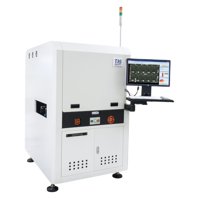
Verify the machine nameplate, camera, factory-set resolution, clearance, optional 3D hardware, software licences and calibration state.
Practical Actions
Close the loop from solder process to inspection
- Stabilize the upstream wave process first: verify flux delivery, preheat, conveyor transfer, alloy condition and wave setup instead of using AOI thresholds to mask process drift.
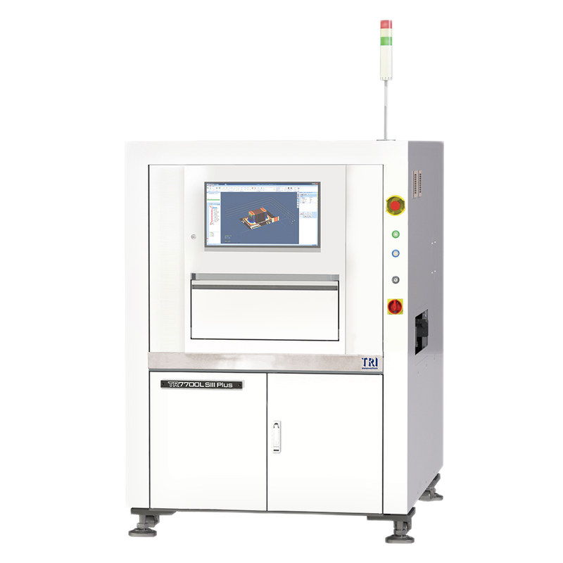
- Separate detection from measurement. Multi-phase 2D imaging can classify many visible defects; height or volume claims require verified 3D hardware, calibration and a suitable view.
- Create golden-board and seeded-defect evidence for the actual product family, then retain program revision, false-call and disposition records.
- Define the response to a flagged board: stop, quarantine, verify, rework or escalate. A detection without a controlled disposition is not a closed loop.
- Ask sellers for a running trial that includes board transfer, optics, program loading, calibration status, defect review and data export.
Common Mistakes
Avoid shortcuts that create false confidence
- Calling every current AOI a 3D AOI when the exact model or option list says otherwise.
- Using a published cm2/s figure as line throughput without the associated resolution, inspection windows and board loading time.
- Expecting top-view AOI to prove hidden bottom-side solder conditions.
- Tuning away false calls without checking whether a solder-process shift caused them.
- Accepting a demo on an unrelated board instead of a representative product and seeded defect set.
Applicability Limits
Know when AOI is not the complete answer
This framework helps evaluate visible assembly and solder defects after wave soldering. It does not establish universal acceptance limits, guarantee defect coverage or replace product-specific standards and process engineering. Hidden joints, internal voids and obstructed bottom-side features may require AXI, electrical test, cross-sectioning or another verified method. The correct route depends on assembly geometry, defect risk and customer criteria.
Technical Sources
TRI: TR7710 official product and inspection specifications